Swan: An open-source C++ software for nanoscale quantum electron transport simulations
Ever wondered why your devices aren’t getting even faster? It turns out, the answer might lie in the tiny details of how metals and semiconductors meet in the transistors. In this project, we’ve built a simulation pipeline including an open-source C++ software based on MPI that allows us to unevil the secrets behind electronic behaviors at the atomic level. Our exploration into the 2D edge contact not only explained the formation of Schottky barriers but also found ways to reduce them effectively.
Read paper »
View code »
The metal-semiconductor contact is a major factor limiting the shrinking of transistor dimension to further increase device performance. In-plane edge contacts have the potential to achieve lower contact resistance due to stronger orbital hybridization compared to conventional top contacts. However, a quantitative understanding of the electron transport properties in the edge contact is still lacking. In this work, we present full-band atomistic quantum transport simulations of the graphene-MoS2 edge contact. By using a Wannier function basis to accurately describe the electronic bands, together with a full self-consistent solution of the electrostatics, we are able to efficiently model device structures on a micron scale, but with atomic level accuracy. We find that the potential barrier created by trapped charges decays fast with distance away from the interface, and is thus thin enough to enable efficient injection of electrons. This results in Ohmic behavior in its I-V characteristics, which agrees with experiments. Our results demonstrate the role played by trapped charges in the formation of a Schottky barrier, and how one can reduce the Schottky barrier height (SBH) by adjusting the relevant parameters of the edge contact system. Our framework can be extended conveniently to incorporate more general nanostructure geometries. For example, a full 3D solution of the electrostatics will also lead to better modeling of the electrical potential. Furthermore, better ab-initio calculations can be conveniently added to our methods to further improve their accuracy.
Results
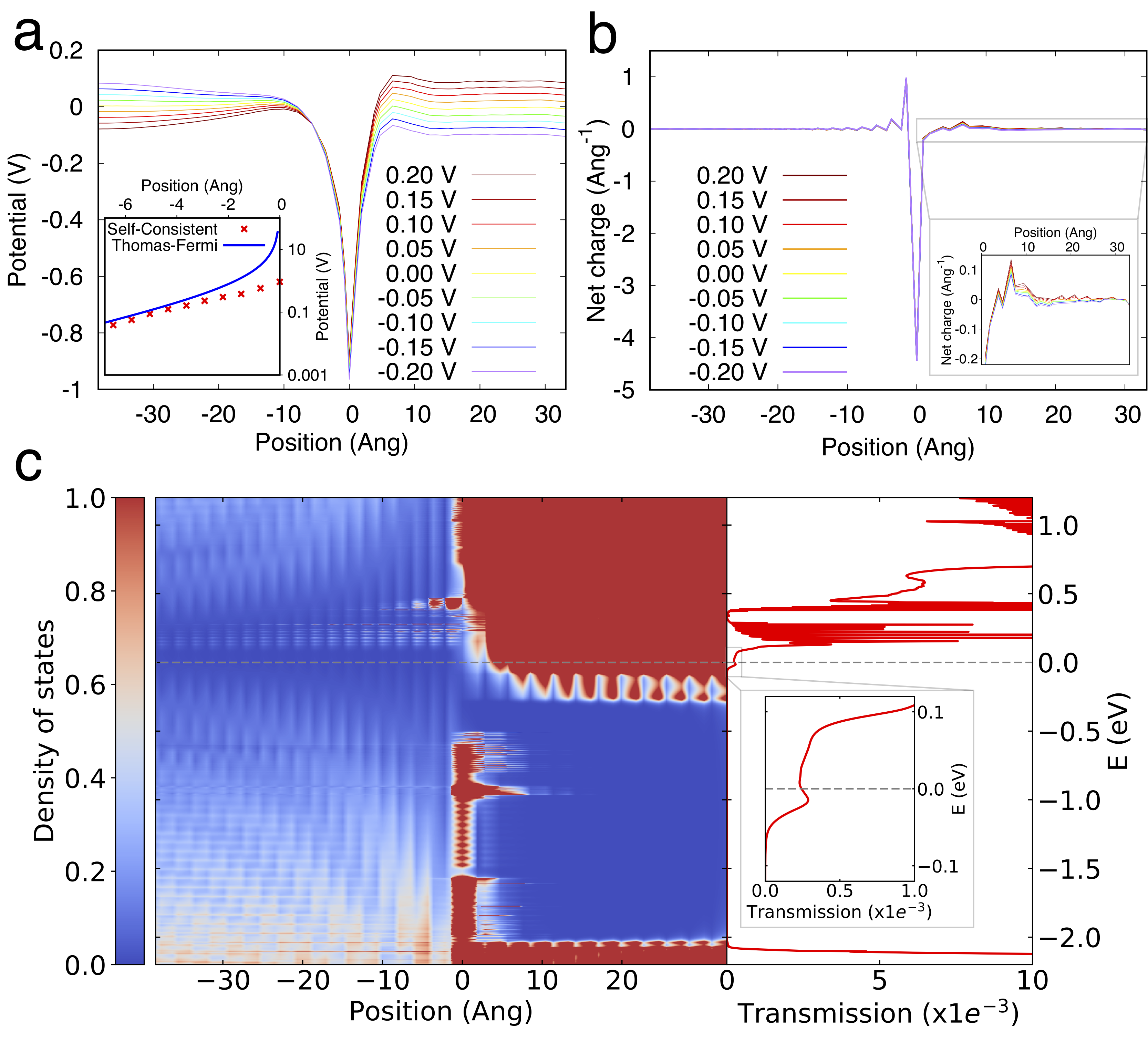
We present in the following results from the above simulation. The first figure shows the converged electrostatic potential and charge density profiles under different voltages. (Inset: comparison between our self-consistent simulation results and analytical predictions using Thomas-Fermi theory.) It also shows the Local Density of States (LDOS) side by side with the transmission spectrum.
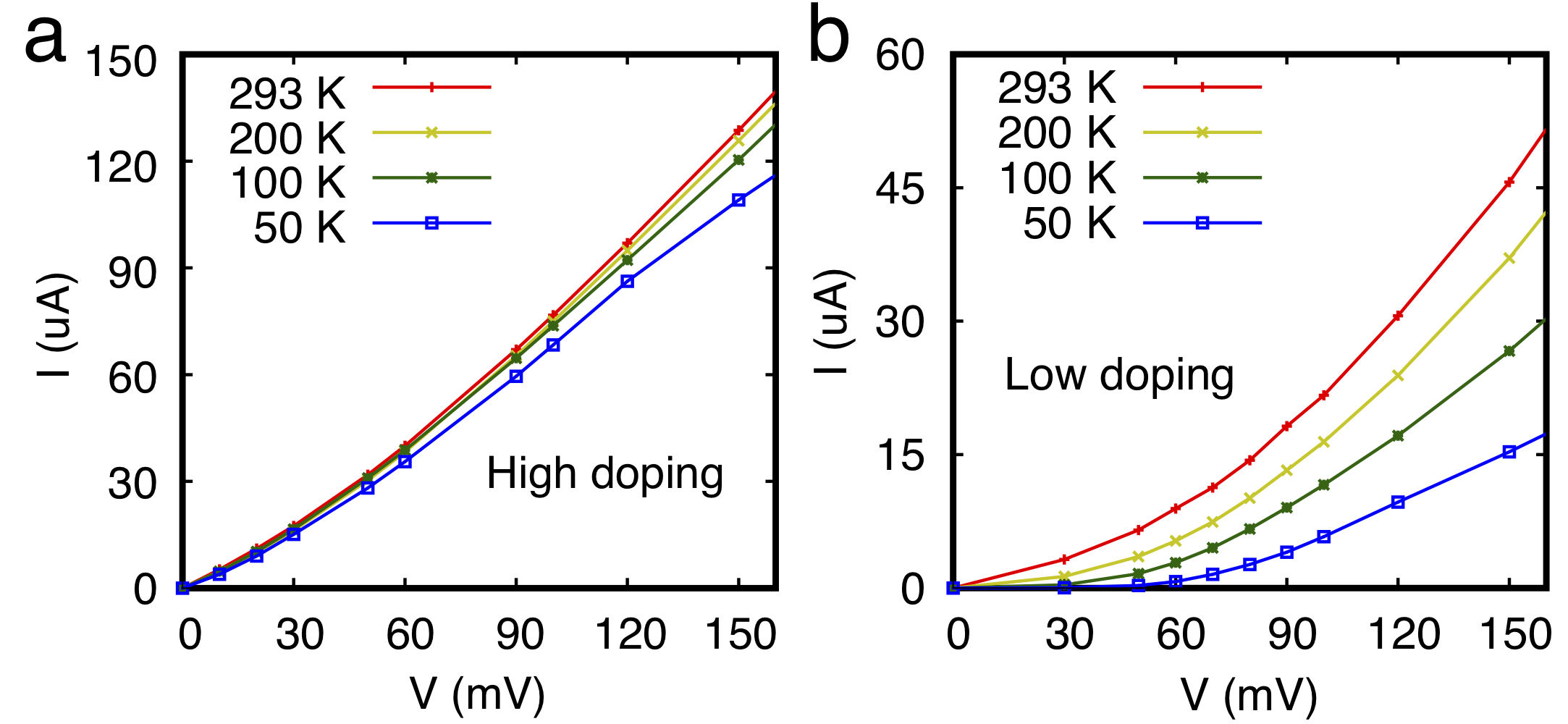
The second one is the I-V characteristics under different temperatures for high and low doping levels respectively. From this figure, one can see the effects of doping on the electron transport behavior of the edge contact device.
Methods
Swan (Self-consistent Wannier-function-based quantum transport solver) is an open-source C++ software suitable for large-scale atomistic simulations of electronic structure and transport properties in nano-devices. The code is available for download on my GitHub page.
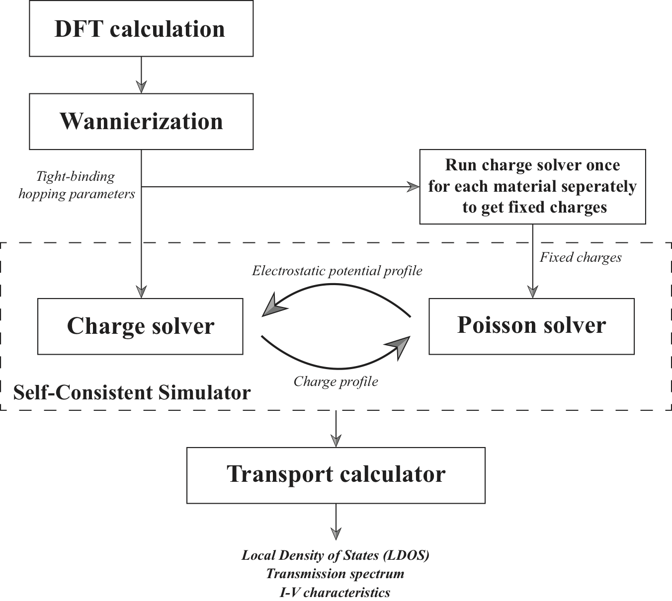
By using a Wannier function basis (as implemented in the Wannier90 package) to accurately describe the electronic bands, our code is able to efficiently model device structures with first-principles accuracy at a minimal cost of tight-binding calculations. It couples the Keldysh non-equilibrium Green’s function formalism and Poisson solver to generate the inhomogeneous charge densities self-consistently with the electrostatic potential profile for the simulated device region. The parallel implementation of the code uses the standard Message Passing Interface (MPI). We depicted our simulation pipeline as below:
Publication
Talks
- W. Dong, P. B. Littlewood, Computational study of quantum electron transport in ohmic edge contacts between two-dimensional materials, American Physical Society (APS) March Meeting. (March 2018)
- W. Dong, P. B. Littlewood, Ab initio simulation of metal contacts to 2D semiconductors with electron-phonon interactions, Materials Research Society (MRS) Spring Meeting. (April 2017)
- W. Dong, P. B. Littlewood, Ab initio simulation of metal contacts to 2D semiconductors with electron-phonon interactions, APS March Meeting. (March 2017)
- W. Dong, A. L. Bezanilla, P. B. Littlewood, Electron transport calculations with Wannier functions in van der Waals heterostructures, APS March Meeting. (March 2016)